Novel Diamond Semiconductors Operate at Highest Power Ever
Researchers
Prof. Makoto Kasu
Niloy Chandra Saha, Toshiyuki Oishi (Saga University),
Seong-Woo Kim (Adamant Namiki Precision Jewel Co., Ltd.)
Abstract
Saga University (SU, President: Hiroaki Kodama) has developed a novel diamond semiconductor whose output power is the highest ever reported for semiconductor devices. The diamond semiconductor devices are deemed to replace vacuum tubes, which are conventionally used in the very-high-frequency and very-high-power applications, leading to increased output power in Beyond-5G wireless base stations, communication satellites, television broadcasting stations, and radar.
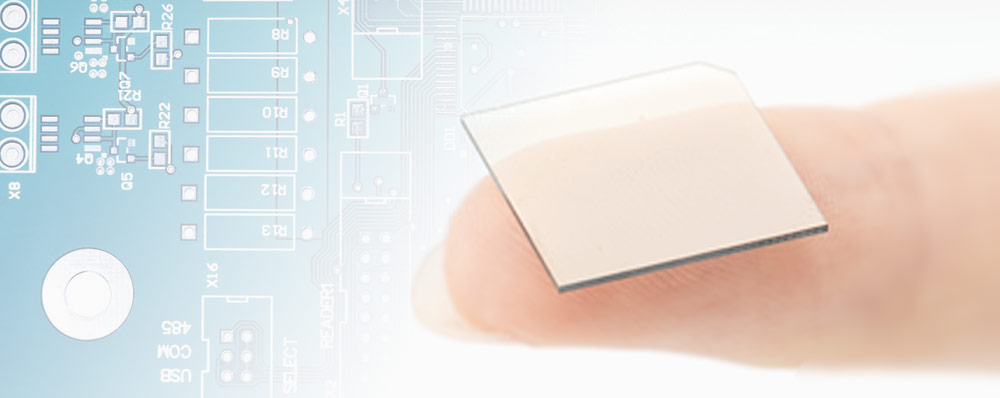
SU, in collaboration with Adamant Namiki Precision Jewel Co., Ltd. (Ad-Na, President: Riyako Namiki), succeeded in fabricating novel diamond semiconductor devices using a wide-scale high-purity diamond wafer.
The diamond semiconductor has gained much attention in recent years as a promising material for the next-generation high-frequency high-power electronics that offers high thermal conductivity, excellent dielectric breakdown field, high carrier lifetime, high saturation carrier velocity due to its high optical phonon energy, and highest electron and hole mobilities. However, despite its impressive properties for power devices, significant improvements are still expected since its current level is much lower, operation lifetime is much shorter than expected, and it remains at the basic research level for decades. Moreover, reliable and large-scale production of diamond crystals remains challenging. Therefore, Ad-Na developed a mass-production technology of high quality, wide-scale, and ultrahigh purity diamond wafers. In addition, SU found a novel principle in the diamond semiconductor device and fabricated these devices, which exhibited drastically increased output power and no degradation phenomenon. Its device power capability is close to silicon carbide (SiC) and gallium nitride (GaN), which dominate the market of power electronic devices and are being developed extensively.
Features
- Diamond semiconductor possessing ultimate power capability
- Mass-production growth technology for wide-scaled high-pure diamond wafer (present: 1 inch)
- Realization of diamond semiconductor devices with a novel principle
- Output power density of 179 MW/cm2, which is the highest ever reported
- Resulting output power density boosts the output power of Beyond-5G base stations and power control in electric car vehicles
- Long-range reliability enables the use of diamond semiconductor devices in space
Background
Recently, there is an increasing demand for high-frequency high-power electronic devices that can operate at high frequencies, which offer higher bandwidth potential, to accommodate the rapid increase of the network capacity of communication networks. Specifically, a portable telephone needs only about 1 W at 1.5 GHz, but communication satellites and television broadcasting stations require 1 kW at 10 GHz, and Beyond-5G communication base stations require 100 W at 100 GHz. In the 10-GHz frequency region, vacuum tubes are still being used for electric power generation and amplification. However, they require a high operating voltage and has a high-power consumption, resulting to a low energy efficiency yield and high energy loss. In contrast, from the environmental viewpoint, these vacuum tubes should be replaced by semiconductors.
Moreover, two important wide bandgap semiconductors suitable for power applications that silicon include silicon carbide (SiC), and gallium nitride (GaN). However, in theory, diamond semiconductor devices exhibit superior physical properties, including high thermal conductivity, high breakdown field strength (1), and high carrier mobility (2), which allow significant reduction of the losses, rapid heat dissipation, and increase in device longevity. Moreover, it can operate 50 000 times higher output-power and energy-efficiency and 1200 times higher frequency than silicon devices, owing to its excellent properties. Therefore, diamond is expected to be the ultimate semiconductor, which is the most suitable for high-frequency high-power electronic devices.
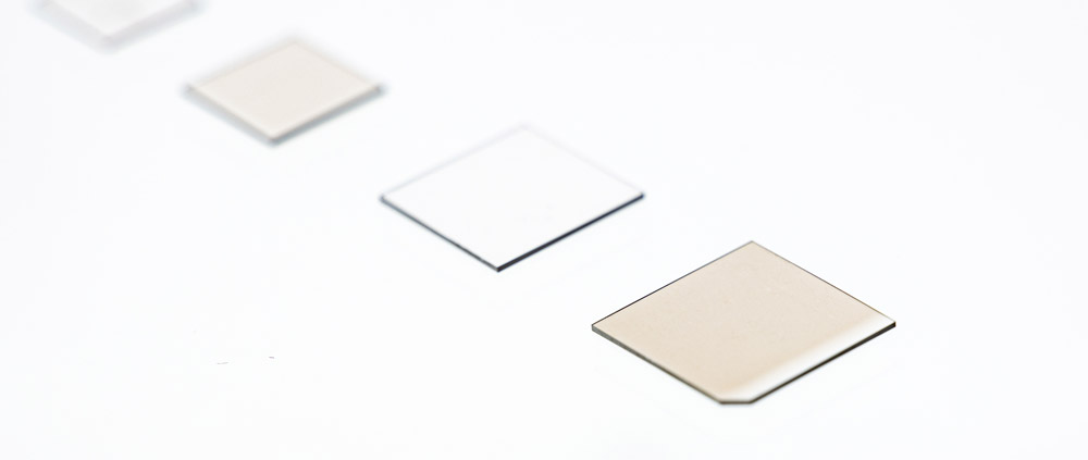
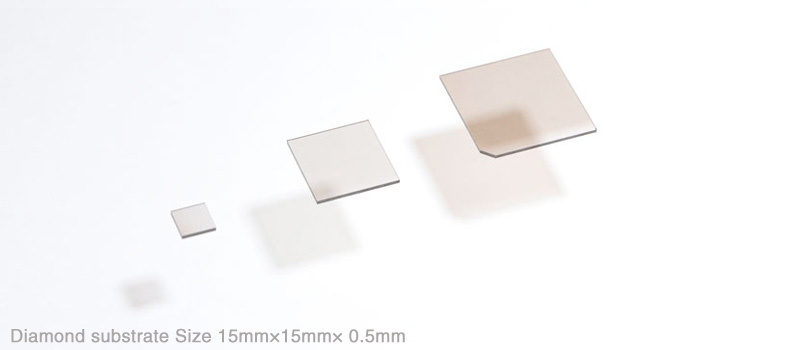
However, high quality and large size wafer of diamonds are needed for industrial applications on electronic semiconductor devices. Thus far, the commercial size of single-crystal diamond plates applied in diamond semiconductor devices is 4 mm in general and degrades faster. Therefore, despite the excellent properties and characteristics of a diamond semiconductor, it is considered to be almost impossible for industrial applications.
Technology
(1) Technology for growing wide-scaled high-pure diamond wafer
As mentioned previously, the commercially available diamond single-crystal plate was limited to 4 mm. However, Ad-Na developed a mass-production technology for growing 1-inch wide-scaled high-pure single-crystal diamond wafers using the microneedle method (*3) on a sapphire substrate. The maximum size of the commercially available sapphire wafer is 6 inches, and therefore the size of the diamond wafer can be expanded up to the maximum sapphire wafer size.
(2) Diamond semiconductor device operated using a novel principle
Up until now, diamond semiconductor devices experience a very low current level and short operation lifetime. In the previous structure, the doping layer (4) that includes the acceptor impurities and the carrier transport layer (4) are close in proximity, affecting the running carriers electrically, and their mobility was limited to an extremely low value. In addition, the chemical reaction of oxygen in the doping layer and hydrogen in the carrier transport layer resulted to a shorter lifetime of the device.
Therefore, we have fabricated the novel structure in which the doping layer is spatially separated from the carrier transport layer by 8 nm. The novel diamond semiconductor device showed high carrier mobility, which is close to the real value. Moreover, its output power density of 179 MW/cm2 is the highest reported in diamond, which is 20 times higher than the previous value. In addition, this value is one order lower than that of GaN, which is being widely developed and used in the industry. For further study, we will be developing premedical technologies to achieve an output power density of 3000 MW/cm2 in the commercial level of Beyond-5G communications.
Future
SU is now developing premedical technologies towards applications in Beyond-5G communications, whose target output power density is 3000 MW/cm2.
Definitions of terms
*1 Breakdown field strength
Semiconductors can be damaged when applying a voltage that is higher than a certain threshold value (i.e., breakdown limit). This phenomenon is called breakdown. The high electric field that limits the occurrence of breakdown is called breakdown field strength, which greatly depends on the type of material used. A material with a high breakdown field strength can be used in high-voltage operation such as in high power semiconductor device. Diamond is a hard material and has a very high breakdown field strength.
*2 Carrier mobility
Carriers are electrons or positive holes, and their velocity governs how a semiconductor device will perform. Intrinsically, diamond material possesses high carrier mobility, resulting to a possible operation of the diamond semiconductor at higher frequencies. Hitherto, the high mobility was drastically limited by impurities.
*3 Microneedle method
In the diamond layer growth, the layer structure with a two-dimensional array of diamond needles with a few microns diameter, a few tens of microns in length, and 10 micron in pitch is fabricated. The layered structure absorbs tension between the diamond and substrate material, enabling the wide-scaled diamond wafer growth. The layered structure with an array of microneedles resembles the Kenzan used in flower arrangement. Thus, the diamond was fabricated using the Kenzan Diamond® method.
*4 Doping and carrier transport layers
For the purpose of generating carriers (electrons or holes), donor or accepter impurities were doped in the layer. This layer is called the doping layer. Meanwhile, the layer in which carriers are being transport is called the carrier transport layer.
Open medium
M. Kasu, et al, “Fabrication of diamond modulation-doped FETs by NO2 delta doping in an Al2O3 gate layer”, Applied Physics Express 14, 051004 (2021). https://doi.org/10.35848/1882-0786/abf445
University Staff Activity DB
https://research.dl.saga-u.ac.jp/profile/ja.2d82a58bcbe158ac.html
For further information please contact:
Makoto Kasu
Department of Electric and Electronic Engineering, Saga University
E-mail address: kasu@cc.saga-u.ac.jp
Tel: +81-952-28-8648
Uchida Hideaki
Adamant Namiki Precision Jewel Co., Ltd.
E-mail address: uchida@orbray.com
Tel: +81-3-3919-2200